
0b688dfe87d71e541a41eac9a34d3287eeaa1ef6.png)


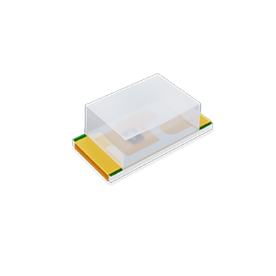
ZOS-T1002-02
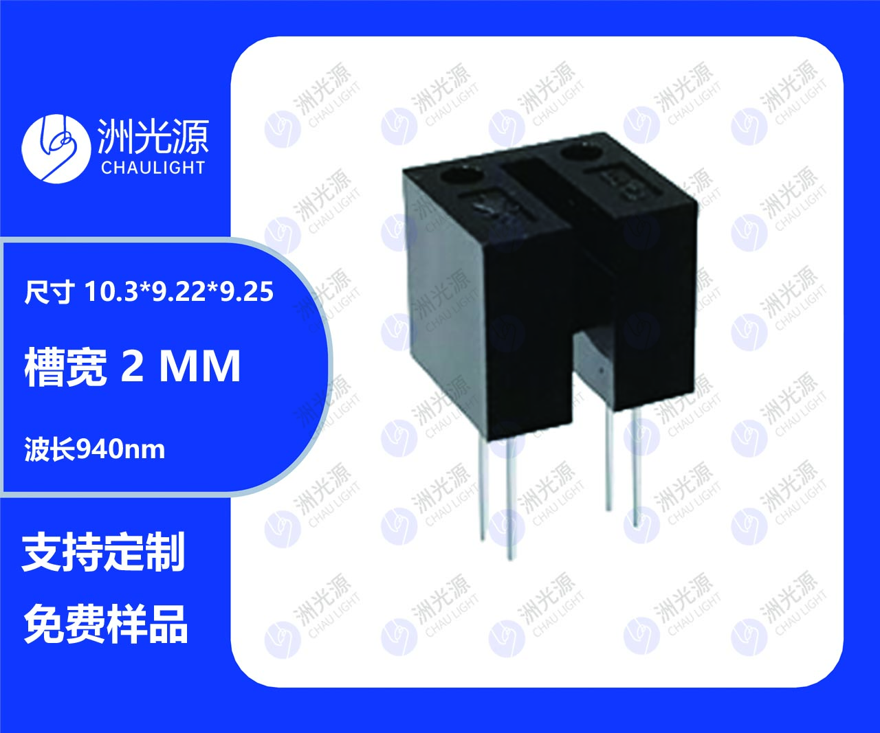
ZOS-T1002-02 由红外发射二极管和 NPN 硅光晶体管组成,它们并排封装在黑 色热塑性外壳中的汇聚光轴上。光电晶体管只接收来自 IR 的辐射。这是正常 情况。但当物体在中间时,光电晶体管不能接收辐射。有关更多组件信息, 请参阅 IR 和 PT。
The ZOS-T1002-02 consist of an infrared emitting diode and an NPN silicon phototransistor, encased side-by-side on converging optical axis in a black thermoplastic housing.The phototransistor receives radiation from the IR
only .This is the normal situation. But when an object is in between , phototransistor could not receives the
radiation.For additional component information , please refer to IR and PT.
产品尺寸 Package Dimension
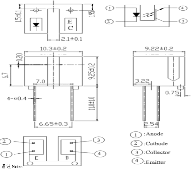
--所有尺寸为毫米标识
All dimensions are in millimeters --未标识尺寸正负公差为 0.3mm
Tolerances unless dimensions ±0.3mm
光电特性 Electro-Optical Characteristics
|
电性参数(温度=25℃) Parameter(Ta=25℃) |
符号 Symbol |
条件 Condition |
最小值 Min. |
典型值 Typ. |
最大值 Max. |
单位 Units |
|
|
输入端 Input |
正向电压 Forward Voltage |
VF |
IF=20mA |
-- |
1.2 |
1.6 |
V |
|
IF=100mA*2 |
-- |
1.4 |
1.85 |
||||
|
IF=1A *2 |
-- |
2.6 |
4.0 |
||||
|
峰值波长 Peak Wavelength |
λp |
IF=20mA |
-- |
940 |
-- |
nm |
|
|
反向电流 Reverse Current |
IR |
VR=5V |
-- |
-- |
10 |
μA |
|
|
输出端 Output |
暗电流 Dark Current |
ICEO |
Ee=0mW/cm2 VCE=20V |
-- |
-- |
100 |
nA |
|
集电极-发射极的工作电压 C-E Saturation Voltage |
VCE(SAT) |
IC=2mA Ee=1mW/cm2 |
-- |
-- |
0.4 |
V |
|
|
转换特性 Transfer Characteristics |
上升时间 Rise Time |
tr |
VCE=5V IC= 1mA RL= 1000Ω |
-- |
15 |
-- |
μS |
|
下降时间 Fall Time |
tf |
-- |
15 |
-- |
|||
|
光电流 Collector Current |
IC(ON) |
IF=20mA VCE=5V |
4.0 |
-- |
20 |
mA |
|
*2 、脉宽少于等于 100us , 占空比 1% Pulse width≦100μs,Duty cycle= 1%
最大额定值 Absolute Maximum Ratings
|
测试项目 Parameter(Ta=25℃) |
符合 Symbol |
范围 Ratings |
单位 Unit |
|
|
输入端发射极 Input Emitter |
功率 Power Dissipation *1 |
Pd |
75 |
mW |
|
反向电压 Reverse Voltage |
VR |
5 |
V |
|
|
持续正向电流 Forward Current |
IF |
50 |
mA |
|
|
脉冲正向电流 Peak Forward Current *2 |
IFP |
1 |
A |
|
|
输出端接收极 Output Detector |
功率 Power Dissipation *1 |
Pd |
75 |
mW |
|
集电极-发射极电压 Collector-Emitter Voltage |
VCEO |
30 |
V |
|
|
发射极-集电极电压 Emitter-Collector Voltage |
VECO |
5 |
V |
|
|
集电极电流 Collector Current |
IC(ON) |
20 |
mA |
|
|
工作温度 Operating Temperature |
Topr |
-25~+85 |
℃ |
|
|
储存温度 Storage Temperature |
Tstg |
-40~+85 |
℃ |
|
|
焊接温度 Lead Soldering Temperature*3 |
Tsol |
260 |
℃ |
|
*1 、 在 25 摄氏度的环境中测试 below 25 Free Air Temperature
*2 、脉宽少于等于 100us , 占空比 1% Pulse width≦100μs,Duty cycle= 1%
*3 、离胶体 2mm 以上焊接 5s 内 2mm form body for 5 seconds